Evaluation video :
Comparison of pattern of silicon wafer from back side
(1100nm vs 1300nm vs 1550nm)
This video shows pattern of silicon wafer from back side. *0sec: Back side Surface of silicon wafer *7sec : 1100nm’s pattern image *16sec : 1100nm’s pattern image after doing image processing. *27sec : 1300nm’s pattern image *38sec : 1550nm’s pattern image
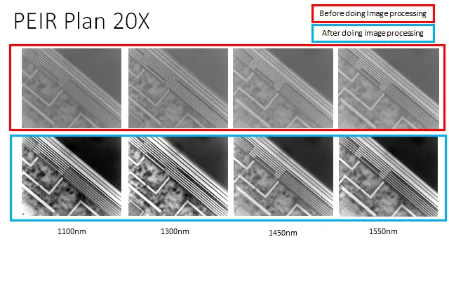
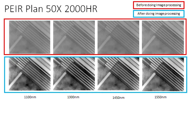
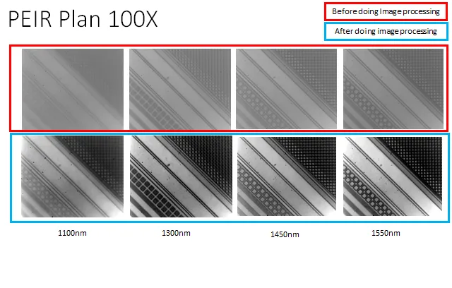
Comparison images of silicon wafer from back side
(1100nm vs 1300nm vs 1450nm vs 1550nm)