Wafer Review Equipment
[Overview]
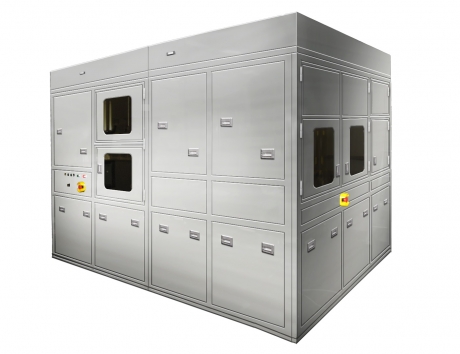
Device for detailed analysis of NG images, storage of analysis data, and communication with host PC based on information provided by wafer inspection system.
[Use]
Defect management in semiconductor device / CMOS device manufacturing process
[Specification]
Applicable work size: 12 inch / 8 inch
————————————————– ————————-
Work state: Wafer dicing
————————————————– ————————-
Stage positioning accuracy: ± 1um
————————————————– ————————-
Review accuracy: 3σ ≤ ± 20um
* Positioning accuracy for defect information coordinates
—————————————————————————
Throughput: Approximately 2000 seconds (10-sheet processing)
* Number of defects: 100 / piece
* Reference imaging mode
* Depends on defect location
—————————————————————————
Review (moving to AF to imaging) time: fastest 0.5 seconds
* Depends on defect location
—————————————————————————
The System takes defect images and the datum are uploaded to the upstream system.
The defect infomation is provided by Wafer Review System and Wafer Inspection System; AVI.
The System also analyzes the defect information from AVI.
Seiwa SAWR Series inspect your application at high speed with high precision.
We can also manufacture AVI.