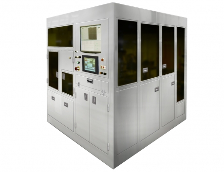
[Overview]
Simultaneously measure the amount of misalignment of the front and back patterns after double-sided exposure and the misalignment of the wafer after bonding from both sides (Top-Bottom measurement).
Measurement of alignment deviation after surface layer exposure (TOP-TOP measurement)
Cassette to cassette type and semi-auto type available.
[Use]
Semiconductor device
CMOS device
Front and back patterning accuracy control in
sensor device manufacturing process
[Specification]
Wafer size Max φ12 inch
————————————————– ——————-
Measurement repeatability 10X 0.2μm / 3σ (Top-Bottom)
20X 0.02μm / 3σ (Top-Bottom)
———————————————————————
Screen measurement location 25 positions
———————————————————————
Recipe number 2,000
———————————————————————
Throughput Top-Top 100 sheets / hour
* 5 points measurement Top-Bottom 100sheets / hour
———————————————————————